ESP32 modules with built-in WiFi/Bluetooth antennas have become very popular. Several of my recent RF EM-simulation projects for clients were about design-in of ESP32 modules in challenging environments. I was excited to see a press release today on the two-antenna version ESP32-WROOM-DA, so I decided to give this concept a quick try even before there are official documents on the actual product.
Looking at the photo in the press release, it seems that both antennas are identical to the single antenna, just rotated by 45° and mirrored. So let’s have a look at the performance and pattern of that approach.
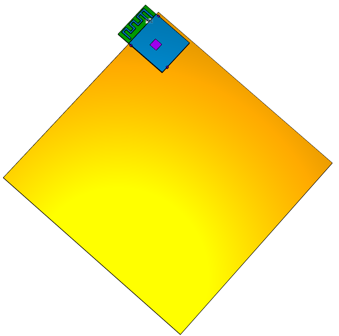
Single antenna case – ESP32-WROOM-32E
As the baseline for our comparison, we use the single antenna module ESP32-WROOM-32E mounted on a 100 mm x 100mm main board. Module position is in the right corner, as recommened in the Hardware Design Guidelines. The main board has a large ground layer, and module ground is connected to main board ground by 3 edge pads and the center ground pads.
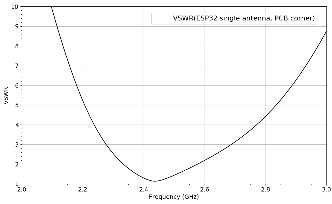
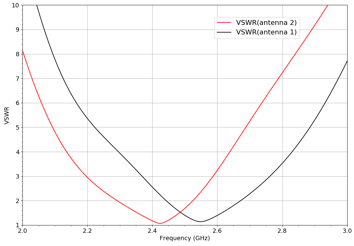
For this placement, we have excellent VSWR with the desired 2.45 GHz center frequency.
The antenna pattern with this placement has several dips (minima), and does not provide the desired omnidirectional pattern. Such a deep minimum across the PCB is found for many antenna designs placed on a PCB corner.
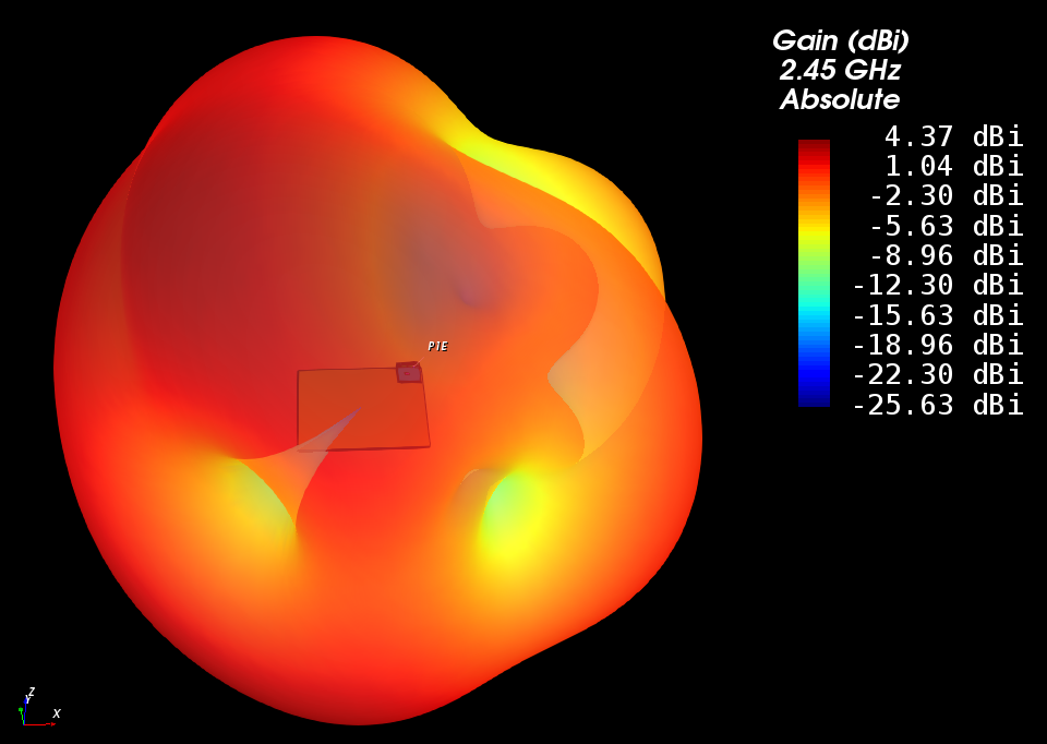
With this pattern in mind, we understand why designers consider a second antenna with 90° rotation.
Adding another antenna – ESP32-WROOM-DA
The dual antenna layout in the press release looks very much like a 45° rotated version, plus a mirrored second antenna. I tried to adopt the antenna ground from the single antenna layout, and convert it to two antenna while maintaining the local ground situation for each radiator. The model below shows my educated guess what the layout and ground looks like:
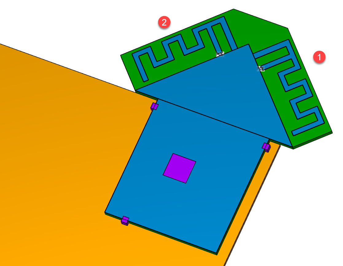
Placement on the corner is the same, we just added the two radiators with keep-out area the same as before. For visualization and simplicity of modelling, module ground = RF ground is drawn on the top layer. In the actual product, RF ground is on a lower layer, but that doesn’t make any difference for simulation.
For the two antenna system, we have two VSWR curves and both are not identical because the local PCB ground environment for both antennas is not the same: the right antenna (1) has its “hot” end of the radiator at the PCB corner, while for the left antenna (2) that is located away from the corner. This causes an offset in resonance frequency.
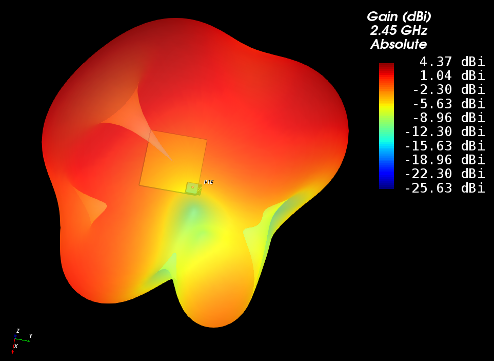
Let’s check the promise of the two-antenna version: can it avoid the deep minima by switching to the other antenna? Here is one view showing the minima of antenna 1, and then the same view with antenna 2:
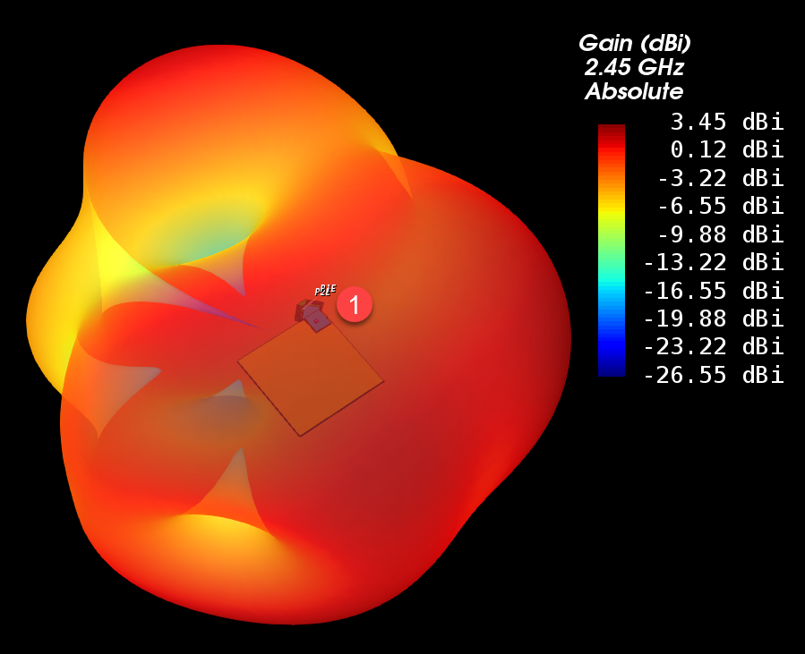
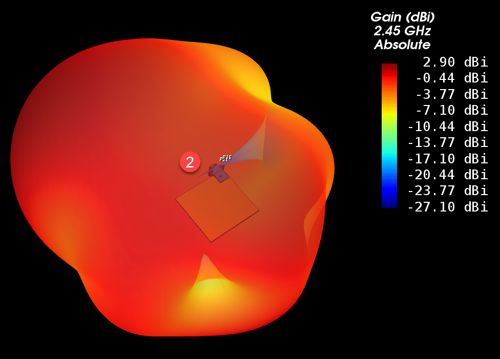
That looks encoraging! Most of the minima with antenna 2 disappear, so switching from one antenna to the other should indeed give improved coverage. Let’s double check with another view:
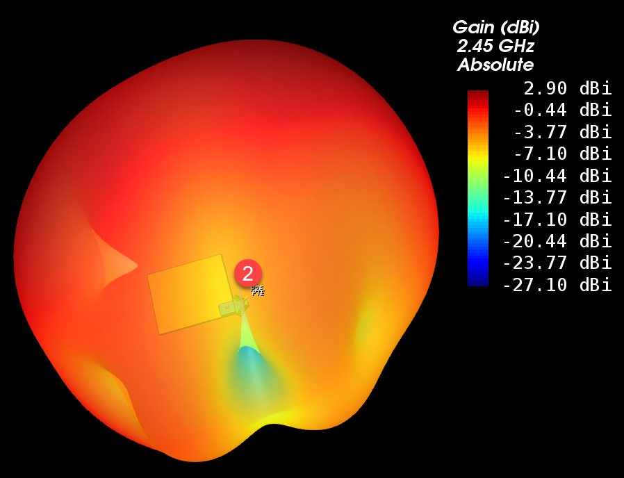

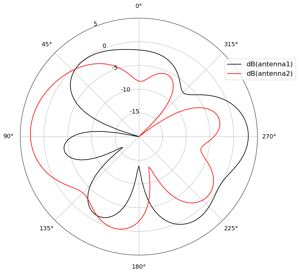
This minimum does not disappear completely, but the signal loss is reduced a lot by switching from antenna 2 to antenna 1. For those of you who are more used to polar plots, here is the antenna pattern in the PCB plane (E_total at theta=90°):
Conclusion
This early investigation confirms that the switched antenna design in ESP32-WROOM-32E makes perfect sense, if the module is placed in a PCB corner. For other placements along the corner, which are not shown here, we find a shift in resonance and minima that are not filled so nicely by antenna switching.
Continue to part 2, which investigates the effect of main board size on antenna matching
3D EM simulations above were done using Empire XPU, a very fast and efficient simulation tool based on FDTD method. As a value-added Empire reseller, we can provide simulation models and evaluation software on request. We also provide consulting services for antenna design and simulation-based optimization of antennas for your specific environment, which might be less ideal than the reference PCB discussed here. We can support you for cases where reference designs fail.
Interested? Please get in touch!